







For decades, making computers faster has depended partly on making the components inside their chips smaller.
Eventually, however, shrinking everything creates a different problem.
The microscopic metal wires connecting billions of transistors become so close together that electrical interactions between them can waste energy and slow the chip down.
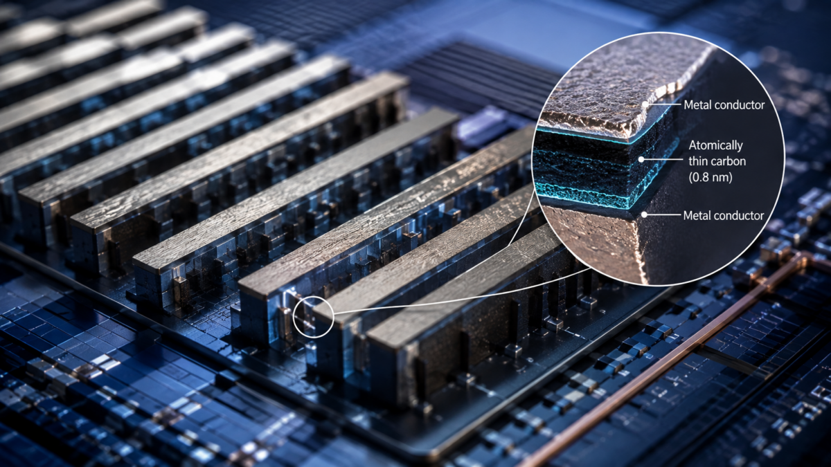
Researchers have now developed an unusual material that could help solve that problem: a layer of amorphous carbon only 0.8 nanometres thick.
That is less than one billionth of a metre.
Despite being extraordinarily thin, the material behaved as a highly effective electrical insulator, resisted breakdown and prevented metal ions from moving through it.
Published in Nature Electronics, the research suggests that an atomically thin form of carbon could eventually replace several layers currently required between the tiny conducting wires inside advanced computer chips.
The spaces between chip wires are becoming a problem
A modern processor is not simply a flat collection of transistors.
Above those transistors sits a complicated network of microscopic metal interconnections that carries electrical signals around the chip.
As manufacturers make those wires smaller and pack them more closely together, unwanted electrical interactions between neighbouring conductors become increasingly important.
This is known as parasitic capacitance.
In simple terms, nearby wires can begin influencing one another electrically even though engineers do not want them to.
This can increase power consumption and contribute to delays as signals move through the chip.
One way of reducing the effect is to place materials with a very low dielectric constant between the wires.
The problem is that many conventional low-dielectric materials become mechanically unstable when engineers try to make them only a few nanometres thick.
The carbon reached a dielectric constant of 1.35
The researchers produced an amorphous carbon material dominated by sp² carbon bonds and tested it at thicknesses ranging down to just 0.8 nanometres.
Its measured dielectric constant was approximately 1.35.
The number matters because a lower dielectric constant means a material is less easily polarised by an electrical field and can therefore reduce unwanted capacitance between neighbouring conductors.
Vacuum has a dielectric constant of one, providing a useful reference point.
The challenge for chip manufacturers is not simply finding a material with a low number.
It also needs to remain physically intact, electrically insulating and manufacturable at extremely small scales.
The new carbon film maintained its ultralow dielectric behaviour across the researchers’ tested thickness range rather than losing its useful properties as it approached the atomic scale.
Being thin is useless if electricity simply breaks through it
An insulating material only works if it can withstand the electrical fields inside a device.
The carbon film demonstrated a dielectric strength of approximately 28 to 31 megavolts per centimetre.
For comparison, the researchers report a value of around 7.3 megavolts per centimetre for amorphous boron nitride, another material investigated for ultrathin electronics.
The carbon was also mechanically hard.
Nano-indentation measurements produced a hardness of around 100 gigapascals, at least an order of magnitude greater than silicon dioxide in the researchers’ comparison.
This combination is important because some materials achieve very low dielectric constants by becoming porous.
Porosity can reduce electrical polarisation, but it can also leave a material mechanically weak.
The new carbon takes a different route.
Its highly disordered atomic structure appears to keep its electrical polarisation unusually low while maintaining considerable physical strength.
It can also stop metal atoms moving where they should not
Chipmakers face another problem as components become smaller.
Metal atoms from conducting lines can gradually diffuse into neighbouring materials.
That movement can eventually degrade the device.
Manufacturers therefore add separate diffusion-barrier layers around metal conductors.
The researchers found that the amorphous carbon film could perform this role as well.
At a thickness of only 0.8 nanometres, its projected time to failure as a metal-ion diffusion barrier exceeded 10 billion seconds.
The study reports that this is more than two orders of magnitude greater than tantalum nitride, an industry-standard barrier material used for comparison.
A single material that both electrically separates neighbouring wires and prevents metal diffusion could be especially useful because every extra layer occupies valuable space inside an increasingly crowded chip.
The carbon could replace several layers with one
Today’s interconnect structures can contain the metal conductor together with insulating material, diffusion barriers, liners and protective layers.
Each component solves a different engineering problem.
But together they take up space.
As the conducting wire becomes narrower, the surrounding layers can consume an increasingly large proportion of the available area.
The researchers suggest that ultralow-k carbon could potentially combine several of these functions into one atomically thin coating.
That would leave more room for the metal conductor itself while reducing the unwanted capacitance between neighbouring lines.
The result could ultimately help reduce what engineers call RC delay, one of the increasingly important limitations affecting the speed of highly scaled electronic circuits.
The researchers grew it across a four-inch wafer
A material can perform beautifully in one microscopic experiment and still be almost useless for semiconductor manufacturing.
One encouraging aspect of the new research is therefore how the carbon was produced.
The team developed a chemical vapour deposition process that allowed them to control the film thickness and grow it across a four-inch wafer.
The process operated at temperatures below 300°C.
It was also able to coat different materials and follow three-dimensional structures, including the sides and bottoms of microscopic trenches.
This conformal growth is important because future chips increasingly contain complicated three-dimensional geometries rather than simple flat surfaces.
The material has not, however, been demonstrated inside a mass-produced commercial processor.
Moving from experimental wafers to a full semiconductor production line remains a substantial engineering challenge.
The next test is whether it survives real chipmaking
The National University of Singapore research team is now working on that transition.
In April 2026, the university began a research collaboration with semiconductor manufacturer TSMC to evaluate the material for ultralow-dielectric insulation and chipmaking applications.
The researchers are also working to scale the deposition process and investigate manufacturing consistency and long-term reliability.
Those tests matter.
A material destined for advanced chips must survive many additional fabrication steps and perform reliably across enormous numbers of components.
The current study demonstrates the underlying material properties rather than proving that commercial processors using the carbon layer are ready for production.
At the atomic scale, the material between the wires matters too
Much of the public discussion around advanced chips focuses on transistors.
How small are they? How many can manufacturers fit onto a processor? How quickly can they switch?
But the billions of transistors inside a modern chip are only useful if they can communicate efficiently.
As electronic components approach atomic dimensions, seemingly mundane materials separating one conductor from another become critical parts of the engineering problem.
A carbon film less than a nanometre thick will not, by itself, create the next generation of processors.
But if it can survive industrial chipmaking while retaining the properties demonstrated in the laboratory, it could remove one of the obstacles standing in the way.
Eventually, keeping computers shrinking may depend just as much on what engineers can squeeze between the wires as on the wires themselves.
Source Information
Study Title: Atomically thin amorphous carbon with an ultralow dielectric constant
Authors: Chee-Tat Toh, Artem K. Grebenko, Ugur Karadeniz, Usha Bhat, Ya He, Hongji Zhang et al.
Journal: Nature Electronics
Published: 18 August 2026
Material thickness: Down to 0.8 nm
Dielectric constant: 1.35 ± 0.10
Dielectric strength: 28–31 MV cm⁻¹
DOI: 10.1038/s41928-026-01685-2