








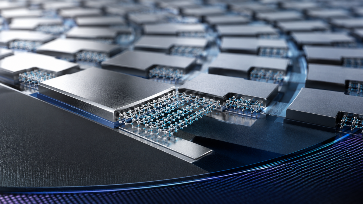
More than 1,000 electronic devices built around molecular layers thinner than one nanometre have been manufactured with working yields reaching as high as 99%.
That matters because molecular electronics has faced an awkward engineering problem for decades. Individual molecules can be designed with useful electrical properties, but incorporating them reliably into the types of structures used in modern electronics has proved considerably more difficult.
Researchers at the Massachusetts Institute of Technology have now demonstrated a manufacturing approach designed to bridge that gap.
Published in Nature Nanotechnology, the research produced more than 1,000 electrically active metal-molecule-metal devices and reported yields of up to 99%. The devices also remained operational over as many as 100,000 measurement cycles.
The problem is not making the molecule
Molecules offer an unusual degree of control at extremely small scales.
Their chemical structure can be deliberately altered, allowing researchers to change properties that influence how they conduct electricity, interact with light or respond to their environment. This has made molecular materials attractive for potential applications ranging from computing and sensors to optical and quantum technologies.
The difficulty comes when those molecules need to become part of an actual device.
Modern semiconductor manufacturing generally relies on top-down processes in which structures are patterned, deposited and etched onto a surface. Those processes work exceptionally well for conventional materials, but the chemicals, heat and physical stresses involved can damage molecular layers.
Instead of forcing the molecules through the full manufacturing process, the MIT researchers reversed part of the sequence.
They first manufactured the supporting device structures using conventional semiconductor fabrication techniques. The molecular material was introduced afterwards, allowing the most delicate part of the device to avoid many of the processes that could otherwise damage it.
The device effectively finishes assembling itself
The technique relies on what the researchers call self-assembled contacts.
After the molecular layer is deposited, carefully engineered surface interactions cause a suspended metal contact to move into position over it. Capillary forces generated as liquid evaporates help bring the structures together, while molecular-scale surface forces stabilise the resulting contact.
This creates an electrical connection without requiring the molecular layer to withstand another aggressive fabrication process.
The researchers were able to use the method with molecular layers measuring less than one nanometre in thickness. In-situ Raman measurements were also used to check whether the molecules remained intact during fabrication, providing evidence that the process had not simply produced working devices by sacrificing the material it was designed to preserve.
For emerging electronics, however, producing one carefully constructed device is only a limited achievement. The more difficult question is whether the process can be repeated.
That is where the reported yield becomes important.
Across more than 1,000 electrically active devices, the researchers achieved yields reaching 99%. Stable operation was demonstrated across as many as 100,000 measurement cycles, suggesting that the approach can produce more than isolated laboratory prototypes.
From individual devices to computing
The team also connected molecular memory devices into a larger array.
Using this system, they demonstrated vector-matrix multiplication, a mathematical operation widely used in computing and particularly important in areas such as neural-network processing and neuromorphic computing.
This does not mean that molecular processors are about to replace silicon chips.
The significance is more specific. Molecular electronics research often concentrates on proving that a particular molecule or individual nanoscale device can perform a useful electronic function. A manufacturing platform becomes more interesting when those devices can also be produced repeatedly and connected into systems.
The new technique begins to address both problems.
It also does so while retaining conventional semiconductor manufacturing for the parts of the process where those established techniques already work well. Rather than proposing an entirely new manufacturing ecosystem, the researchers are combining top-down fabrication with bottom-up molecular assembly.
Smaller does not automatically mean better
Molecular materials still face substantial hurdles before they could become routine components in commercial electronics.
Performance, long-term reliability, manufacturing cost, integration with existing circuitry and the ability to produce much larger systems will all matter. A laboratory demonstration of more than 1,000 devices remains far removed from the enormous manufacturing scale of contemporary semiconductor production.
The researchers are therefore presenting the technique as a platform for developing and testing new classes of molecular and atomic-scale devices, rather than as a replacement for today’s processors.
But the distinction is important.
The challenge in future electronics is increasingly not simply whether researchers can create useful behaviour at extremely small scales. It is whether that behaviour can survive the transition from an interesting material to a repeatable device and, eventually, to a functioning system.
A 99% yield across more than 1,000 molecular devices suggests that transition may be becoming considerably more practical.
Source Information
Study title: Self-assembled contacts for high-yield molecular devices
Authors: Sarah O. Spector, Peter F. Satterthwaite, Maxwell Conte, Teddy Hsieh, Eduard O. Bobylev, Kieran Dunn, Weikun Zhu, Jinwoo Sim, Jeremiah A. Johnson and Farnaz Niroui
Journal: Nature Nanotechnology
Published: 3 August 2026
DOI: 10.1038/s41565-026-02227-9